


- Mark as New
- Bookmark
- Subscribe
- Mute
- Subscribe to RSS Feed
- Permalink
- Report Inappropriate Content
Hi,
I have a question towards the SLWR and SLCS timing in the master side GPIFII interface.
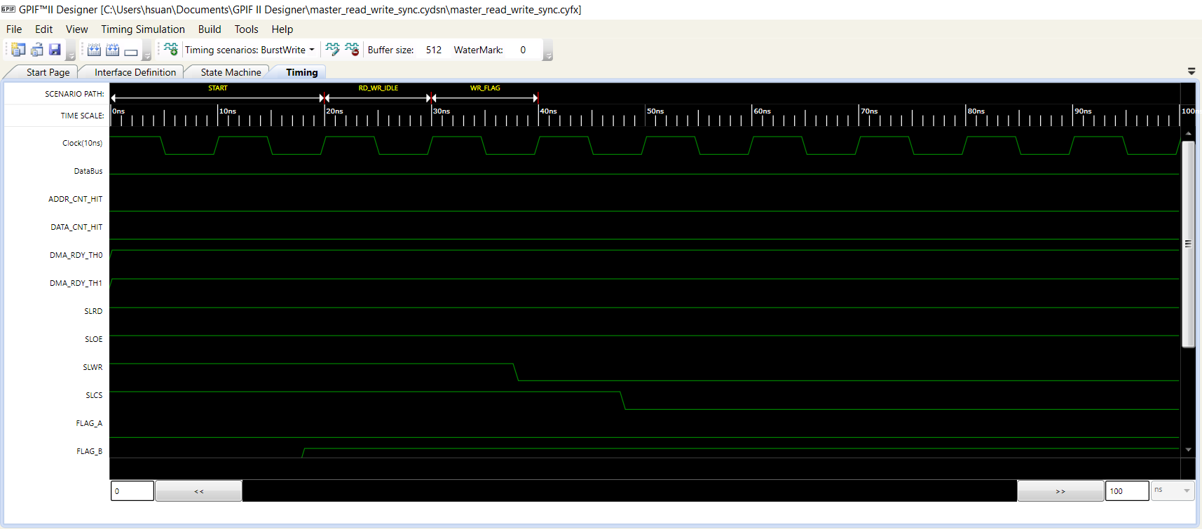
In Figure 6. of the AN82716, the SLCS signal becomes low and then the SLWR signal becomes low.
I've also attached the snapshot of the figure in attachment.
The timing diagram of the GPIFII designer project of the master side shows the SLWR comes low before the SLCS signal.
Please see the attached master_gpif2_designer file.
Is there anything I misunderstand?
Thanks,
Jay
Solved! Go to Solution.
- Mark as New
- Bookmark
- Subscribe
- Mute
- Subscribe to RSS Feed
- Permalink
- Report Inappropriate Content
Hi,
There is a parameter in the GPIF Designer : OUTPUT VALUE which affects the way in which a GPIO is asserted and when it is shown as asserted.
So, if a GPIO is configured as EARLY, there is a latency of 2 clock cycles for it to show in the timing diagram from the point it is asserted,
And, if a GPIO is configured as DELAYED, there is a latency of 3 clock for it to show from the moment it is asserted in the state machine.
In the master state machine, SLWR is early and SLCS is delayed, and hence there is a difference in the timing diagram as you have observed.
Please refer to the document :
C:\Program Files (x86)\Cypress\EZ-USB FX3 SDK\1.3\doc\GPIFII_Designer\gpif2_designer_userguide.pdf for more insight into the configuration
Regards,
Yashwant