

- Mark as New
- Bookmark
- Subscribe
- Mute
- Subscribe to RSS Feed
- Permalink
- Report Inappropriate Content
Hi ,
I have one question Is there any method to check if the device is returned from Backup Domain. I am working on device in which Backup domain is required for time tracking and other implementations.
I have looked into Technical Reference Manual Section for Backup Systems and Power Supply where I found VDDBAK_CTL for switching the Power rail between VDDD and VDDBAK.
I also looked into Registers Technical Reference Manual for Backup System Registers BACKUP_STATUS But it only tells the status of WCO and RTC_Busy not if system is returned from BACKUP domain
I also tried to look into Pdl reference manual no API found that could help me.
Kindly help me with the situation
Solved! Go to Solution.
- Labels:
-
PSoC 6 MCU
- Tags:
- backup domain
- psoc 6
- Mark as New
- Bookmark
- Subscribe
- Mute
- Subscribe to RSS Feed
- Permalink
- Report Inappropriate Content
Hi,
The Backup domain adds an “always-on” functionality to PSoC 6 MCUs using a separate power domain supplied by a backup supply (VBACKUP) such as a battery or supercapacitor. It means as long as the supply is available for the VBACKUP, BACKUP domain will be always operating.
There is no other way to indicate that the BACKUP domain is ON other than reading the data stored in the BACKUP is retained even after the MCU has gone into hibernate mode. When MCU enters hibernate mode the registers other than the BACKUP registers will reset.
So, it is important that supply to the backup pin is always available.
Please, let me know if you need further clarification.
Thank you
Best Regards
Raj Chaudhari
- Mark as New
- Bookmark
- Subscribe
- Mute
- Subscribe to RSS Feed
- Permalink
- Report Inappropriate Content
Hi Raj,
I got what you mentioned above in your reply. But is there any method to read V_BACKUP. I studied the Technical Reference Manual and found we can read V_backup using ADC attached to AMUXBUS-A by setting VBACKUP_MEAS bit in BACKUP_CTL.
I tried to perform the implementation but currently unable to read the correct voltages. Below is my code snippet:
#define ADC_DESIRED_FREQUENCY 8000000 //!< This value is the desired ADC Frequency
#define CONFIG1_CHAN_EN (1u) //!< Enable only channel 0.
// Channel 0 is single ended.
#define CONFIG1_CHAN0_CONFIG (CY_SAR_CHAN_SINGLE_ENDED \
| CY_SAR_CHAN_SAMPLE_TIME_0 \
| CY_SAR_POS_PORT_ADDR_SARMUX_VIRT \
| CY_SAR_CHAN_AVG_ENABLE \
)
// Single ended channels are signed.
// Averaging mode is set to sequential fixed with 32 samples of averaging.
#define CONFIG1_SAMPLE_CTRL (CY_SAR_SINGLE_ENDED_SIGNED \
| CY_SAR_AVG_CNT_32 \
| CY_SAR_AVG_MODE_SEQUENTIAL_FIXED\
| CY_SAR_TRIGGER_MODE_FW_ONLY )
// Channels 1 through 15 are unconfigured.
#define CONFIG1_CHAN_CONFIG {(uint32_t)CONFIG1_CHAN0_CONFIG \
, 0uL, 0uL,0uL,0uL,0uL,0uL,0uL,0uL,0uL,0uL,0uL,0uL,0uL,0uL,0uL}
// Enable the End of Scan interrupt only.
#define CONFIG1_INTR_MASK (CY_SAR_INTR_EOS_MASK)// Enable the bypass capacitor connection.
// Connect the negative terminal for single ended channels to VSSA.
#define CONFIG1_VREF_MV_VALUE (3300uL)
#define CONFIG1_CTRL (CY_SAR_VREF_SEL_VDDA \
| CY_SAR_BYPASS_CAP_ENABLE \
| CY_SAR_SARSEQ_SWITCH_ENABLE )
// Config1 will operate in single shot mode.
// Set the sample time to meet the DieTemp settling time requirement of 1 us.
// With a 16.67 MHz SAR clock, 17 cycles (or a value of 18 in the register)
// gives an aperture time of 1.02 us.
#define CONFIG1_SAMPLE_TIME01 ((8 << CY_SAR_SAMPLE_TIME0_SHIFT) \
| (4 << CY_SAR_SAMPLE_TIME1_SHIFT))
// Set the sample times for 2 and 3 to be 4 clock cycles.
// Note that these two sample times are not used by any channels and only shown for reference.
#define CONFIG1_SAMPLE_TIME23 ((4 << CY_SAR_SAMPLE_TIME2_SHIFT) \
| (4 << CY_SAR_SAMPLE_TIME3_SHIFT))
// Set the initial state of switches.
// Close the switch between the DieTemp sensor and the positive terminal of the SAR (TEMP_VPLUS).
// Close the switch between VSSA and the negative terminal of the SAR (VSSA_VMINUS).
#define CONFIG1_MUX_SWITCH0 (CY_SAR_MUX_FW_VSSA_VMINUS \
| CY_SAR_MUX_FW_AMUXBUSA_VPLUS)
// Enable sequencer control for the VSSA and TEMP switches.
// While unnecessary in this design because there is only one channel in Config1,
// the code is provided for reference for designs with multiple channels.
#define CONFIG1_MUX_SWITCH_SQ_CTRL (CY_SAR_MUX_SQ_CTRL_VSSA \
| CY_SAR_MUX_SQ_CTRL_AMUXBUSA)
#define WAIT_LOOP_TIME 50000
//==============================================================================
// LOCAL DATA STRUCTURE DEFINITION
//==============================================================================
/*******************************************************************************
* Constants for configuring Config1 of the Scan_ADC
*******************************************************************************/
// Define the initialization structure for Config1.
const cy_stc_sar_config_t config1 =
{
.ctrl = (uint32_t)CONFIG1_CTRL,
.sampleCtrl = (uint32_t)CONFIG1_SAMPLE_CTRL,
.sampleTime01 = CONFIG1_SAMPLE_TIME01,
.sampleTime23 = CONFIG1_SAMPLE_TIME23,
.rangeThres = CY_SAR_DEINIT,
.rangeCond = CY_SAR_RANGE_COND_BELOW,
.chanEn = CONFIG1_CHAN_EN,
.chanConfig = CONFIG1_CHAN_CONFIG,
.intrMask = CONFIG1_INTR_MASK,
.satIntrMask = CY_SAR_DEINIT, // Disable the saturation interrupt.
.rangeIntrMask = CY_SAR_DEINIT, // Disable the range interrupt.
.muxSwitch = CONFIG1_MUX_SWITCH0,
.muxSwitchSqCtrl = CONFIG1_MUX_SWITCH_SQ_CTRL,
.configRouting = true,
.vrefMvValue = CONFIG1_VREF_MV_VALUE,
};
int main(void)
{
cy_rslt_t result;
int32_t waitLoop = 0u;
int VBack_voltage = 0;
/* Initialize the device and board peripherals */
result = cybsp_init() ;
if (result != CY_RSLT_SUCCESS)
{
CY_ASSERT(0);
}
/* Enable global interrupts */
__enable_irq();
/* Initialize retarget-io to use the debug UART port */
result = cy_retarget_io_init(CYBSP_DEBUG_UART_TX, CYBSP_DEBUG_UART_RX,
CY_RETARGET_IO_BAUDRATE);
/* retarget-io init failed. Stop program execution */
if (result != CY_RSLT_SUCCESS)
{
CY_ASSERT(0);
}
/* Print message */
/* \x1b[2J\x1b[;H - ANSI ESC sequence for clear screen */
printf("\x1b[2J\x1b[;H");
printf("-----------------------------------------------------------\r\n");
printf("PSoC 6 MCU: ADC using PDL\r\n");
printf("-----------------------------------------------------------\r\n\n");
(void) Cy_SysAnalog_Init(&Cy_SysAnalog_Fast_Local);
Cy_SysAnalog_VrefSelect(CY_SYSANALOG_VREF_SOURCE_LOCAL_1_2V);
/* Turn on the hardware block. */
Cy_SysAnalog_Enable();
// Get peripheral Frequency
uint32_t clkPerifreq = Cy_SysClk_ClkPeriGetFrequency();
// Desired frequency for ADC
uint32_t divider = clkPerifreq / ADC_DESIRED_FREQUENCY;
// Assign the peripheral divider
Cy_SysClk_PeriphAssignDivider(PCLK_PASS_CLOCK_SAR, CY_SYSCLK_DIV_8_BIT, 0u);
/* Divide the PeriClk by 3, which is a input value of 2. */
Cy_SysClk_PeriphSetDivider(CY_SYSCLK_DIV_8_BIT, 0u, (divider-1));
/* Enable the divider. */
Cy_SysClk_PeriphEnableDivider(CY_SYSCLK_DIV_8_BIT, 0u);
// Initialize the ADC Module
Cy_SAR_Init(SAR, &config1);
// Enable the SAR
Cy_SAR_Enable(SAR);
Cy_SysPm_BackupEnableVoltageMeasurement();
for (;;)
{
Cy_SAR_StopConvert(SAR);
Cy_SAR_DeInit(SAR, true);
Cy_SAR_Init(SAR, &config1);
Cy_SAR_Enable(SAR);
// Start the conversion
Cy_SAR_StartConvert(SAR, CY_SAR_START_CONVERT_SINGLE_SHOT );
Cy_SysLib_DelayUs(25);
// Wait for the completion of the conversion cycle
while ((CY_SAR_SUCCESS == Cy_SAR_IsEndConversion(SAR, CY_SAR_RETURN_STATUS)) && (++waitLoop <= WAIT_LOOP_TIME))
{
}
VBack_voltage = Cy_SAR_GetResult16(SAR, 0);
printf("Value read %d\r\n",VBack_voltage);
Cy_SysLib_Delay(1000);
}
}
Thank you
Best Regards
Muhammad Ahtasham Baig
- Mark as New
- Bookmark
- Subscribe
- Mute
- Subscribe to RSS Feed
- Permalink
- Report Inappropriate Content
Hi I hope you are good as I am still looking for solution I want to add some changes I tried. I found an article on cypress explaining routing non-dedicated pin to AMUXBUS link below:
I also got an other example code for testing:
Using this code I tried to read VBACKUP but got constant output as ADC counts between 180-190
I discharged supercapacitor but still same output. I also tried to route non-dedicated pins got similar result
Regards
Muhammad Ahtasham Baig
- Mark as New
- Bookmark
- Subscribe
- Mute
- Subscribe to RSS Feed
- Permalink
- Report Inappropriate Content
Hi I wanted to update you on my working I am able read V_backup using AMUXBUS-A the issue I noticed for configuration not getting applied from device configurator in ModusToolbox, However currently I am using BGR as reference for other references I am getting saturated values . Also on AMUXBUS-A I am getting an Offset at 0 V I get 773 as ADC count
- Mark as New
- Bookmark
- Subscribe
- Mute
- Subscribe to RSS Feed
- Permalink
- Report Inappropriate Content
Hi @AhtashamBaig,
1) I tried the above code mentioned in:
and it is working perfectly fine for me. I just want to ask which one you finally implemented.
2) As you mentioned you are getting the offset at 0V for AMUXBUS-A. Which signal are you driving through the AMUXBUS-A.
Please, share your project. So, I can debug it.
Thank you
Best Regards
Raj Chaudhari

- Mark as New
- Bookmark
- Subscribe
- Mute
- Subscribe to RSS Feed
- Permalink
- Report Inappropriate Content
- Mark as New
- Bookmark
- Subscribe
- Mute
- Subscribe to RSS Feed
- Permalink
- Report Inappropriate Content
Hi @AhtashamBaig,
I have gone through the attached code. But I need more information:
1) What is the exact purpose of this code?
2) What issues you are facing?
3) Are you trying to measure backup voltage or voltage from other GPIO pins?
Please, provide the above information.
Thank you
Best Regards
Raj Chaudhari
- Mark as New
- Bookmark
- Subscribe
- Mute
- Subscribe to RSS Feed
- Permalink
- Report Inappropriate Content
Hi @Raj_C
As mentioned in your next reply I am currently trying to read Backup Voltage from Vbackup attached to SuperCap.
The issue i am getting is for not getting proper ADC count at 0 it returns 773 and At max it returns 1998 3.3 V
I am trying to resolve this issue so i can get proper ADC counts also use External reference attached to VREF which is 3.0 Volts
Regards
- Mark as New
- Bookmark
- Subscribe
- Mute
- Subscribe to RSS Feed
- Permalink
- Report Inappropriate Content
Hi @AhtashamBaig,
I have created the MTB project for Backup voltage measurement (referring to the above PSoC Creator Project).
Cy_SysPm_BackupEnableVoltageMeasurement:
This function enables Vbackup supply measurement by the ADC. The function connects the Vbackup supply to AMuxBusA. The ADC input can then be connected to AMuxBusA. Note that the measured signal is scaled by 10% to allow full range measurement by the ADC. So, scaled it back to real values.
I am using PSoC 62 Wifi-BT kit and it has physical switch to switch between VDDD and supercap for the backup supply voltage and they are getting measured accurately. (Cross verified with Digital Multimeter)
Let me know if this helps with your query.
Thank you
Best Regards
Raj Chaudhari
- Mark as New
- Bookmark
- Subscribe
- Mute
- Subscribe to RSS Feed
- Permalink
- Report Inappropriate Content
Hi
@Raj_C , I tried your code it is similar to my implementation but I am getting wrong output at 0 I am getting 700 and 2013 at 2.0 volts i am attaching my project. I am attaching my project with post hope you can help me with it, Also I tried to read Backup voltage I am able to notice linear change by reading Supercap but it only gives me RAW ADC upto 1200 at 2.8 Volt above it get saturated and returns raw count from 600+.
I hope you understands the issue :
First issue is with wrong reading for saturation it should be reading from 0-3.3V
Second for Supercap it is not giving proper read counts and gives saturated value above 2.8
- Mark as New
- Bookmark
- Subscribe
- Mute
- Subscribe to RSS Feed
- Permalink
- Report Inappropriate Content
Hi @AhtashamBaig,
1) I have found that you are sampling channel 2 but you have configured:
#define CHANNEL_CONFIG {(uint32_t)CHANNEL_0_CONFIG ,0uL,0uL,0uL,0uL,0uL,0uL,0uL,0uL,0uL,0uL,0uL,0uL,0uL,0uL} /* Channels 3 through 15 are unconfigured. */
instead of
#define CHANNEL_CONFIG {0uL,0uL,(uint32_t)CHANNEL_0_CONFIG,0uL,0uL,0uL,0uL,0uL,0uL,0uL,0uL,0uL,0uL,0uL,0uL} /* Channels 3 through 15 are unconfigured. */
2) I have modified CONFIG1_CTRL for external VREF. It takes external voltage from the VREF pin.
#define CONFIG1_CTRL (CY_SAR_VREF_SEL_EXT \
| CY_SAR_BYPASS_CAP_ENABLE)
3) I am able to measure 0 to 3.3 V from pin 9.7 according to your main.c file. (See the attached image)
4) Also add a small delay before starting the ADC conversion.
5) Update the mtb-pdl-cat1 and mtb-hal-cat1 to the latest release in your project library.
I have one question regarding the BACKUP voltage measurement. Which implementation are you using for this?
Please, let me know if the above steps help you and how you are implementing backup voltage measurement.
Thank you
Best Regards
Raj Chaudhari
- Mark as New
- Bookmark
- Subscribe
- Mute
- Subscribe to RSS Feed
- Permalink
- Report Inappropriate Content
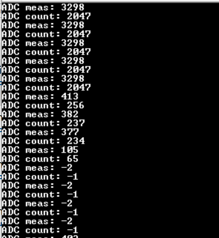
Hi @Raj_C
I tried the changes you mentioned but I am still unable to get voltages properly as at 1.8V+ I get 2047 ADC counts which on conversion getting 3298mV in firmware, I tried with All VREF but results are same.
For the question for implementation of Backup Voltage it has an Supercap attached I discharge it to test the voltage but voltages on DMM and voltages calculated via firmware are different.
I have confusion for Channel configuration Array what is the orientation of channels selection as using Technical reference manual, I observe there are 14 channels attached to SARMUX also can you provide me with any link address explaining the Channel configuration of ADC for PDL, I have gone through PDL library, Technical reference manual and also Application notes

Also I think the issue on my side is for Generated sources they are not correctly working, I also updated my libraries to latest Pdl 2.3.1 and Hal 2.0.1. If Possible can you please send me complete project of yours so I can check the device configuration or differences in generated sources for ADC
Regards,
- Mark as New
- Bookmark
- Subscribe
- Mute
- Subscribe to RSS Feed
- Permalink
- Report Inappropriate Content
Let's take this out of the community for now and I'll submit a support ticket.
- Mark as New
- Bookmark
- Subscribe
- Mute
- Subscribe to RSS Feed
- Permalink
- Report Inappropriate Content
I hope you are doing greater, I wanted to know if you can provide any update on my issue. I didn't got any email that you have started looking into the issue
Regards