


- Mark as New
- Bookmark
- Subscribe
- Mute
- Subscribe to RSS Feed
- Permalink
- Report Inappropriate Content
Hi Guys,
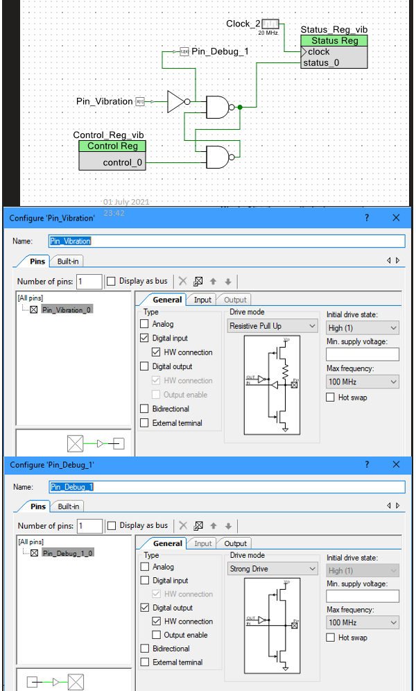
I cannot understand why I am not able to input into the board the signal at PIN_Vibration (see attached circuit).
If all was working Pin_Debug_1 would be following (inverted) Pin_Vibration.

Solved! Go to Solution.
- Labels:
-
PSoC 6 MCU
- Mark as New
- Bookmark
- Subscribe
- Mute
- Subscribe to RSS Feed
- Permalink
- Report Inappropriate Content
Hi,
Reading your
>P8 to which I had attached all this I/O was faulty!
I checked the schematic of CY8CKIT-062-BLE and found the following

In the schematic, "No Load" means that the part is not installed.
And it seems that in J20 P8_0, ... P8_7 are not connected
unless you install (solder) 0 ohm resistors.
So the good news is that "Cypress" knew this from the first place,
the bad news is that I (we) did not noticed that the pin was P8_x... >_<
moto
- Mark as New
- Bookmark
- Subscribe
- Mute
- Subscribe to RSS Feed
- Permalink
- Report Inappropriate Content
Hi,
It would be nice if you can describe the problem more clearly, is it
(1) You can not compile the project
(2) Project can be compiled but Pin_Debug_1 does not output the inverted input signal
(3) Something else
Meantime, please specify the device and/or board you are using.
And if you can, attaching a project with which we can reproduce the problem
usually helps us to determine the problem faster.
Having written above, seeing your schematic, seeing an asynchronous feedback
makes me a little concerned. In the world of ASIC and FPGA, a circuit which has
asynchronous feedback logic often suggest a problematic result.
I wonder if you can replace that part with a D Flip Flop w/ Enable?

moto
- Mark as New
- Bookmark
- Subscribe
- Mute
- Subscribe to RSS Feed
- Permalink
- Report Inappropriate Content
#2 is correct answer.
Sorry for the brevity but I thought mentioning a hardware problem would mean that compilation is ok.
I am using PSoC 6 BLE Pioneer Board.
Actually originally I had a D flipflop doing the job (as I now have it), but turned it into cross coupled nand gates for simplifying the problem from gate count point of view..
The double inverters you now see are there just to let me have a scope probe point. There may be simper ways.

Many thanks.
Stephen.
- Mark as New
- Bookmark
- Subscribe
- Mute
- Subscribe to RSS Feed
- Permalink
- Report Inappropriate Content
Got it!
P8 to which I had attached all this I/O was faulty!
After transferring the pins to another port all worked ok.
Just a humble note, since this outcome would not easily be suspected by an ordinary user like me, I would have appreciated if a Cypress source could have pointed me to it's possibility, it would have saved me a tone of time and hair pulling 😄.
- Mark as New
- Bookmark
- Subscribe
- Mute
- Subscribe to RSS Feed
- Permalink
- Report Inappropriate Content
Please check the board schematic. Some pins have special purpose, and may have, for example, a capacitor or a pull-up resistor attached to it.
- Mark as New
- Bookmark
- Subscribe
- Mute
- Subscribe to RSS Feed
- Permalink
- Report Inappropriate Content
Hi,
Reading your
>P8 to which I had attached all this I/O was faulty!
I checked the schematic of CY8CKIT-062-BLE and found the following
In the schematic, "No Load" means that the part is not installed.
And it seems that in J20 P8_0, ... P8_7 are not connected
unless you install (solder) 0 ohm resistors.
So the good news is that "Cypress" knew this from the first place,
the bad news is that I (we) did not noticed that the pin was P8_x... >_<
moto