- Mark as New
- Bookmark
- Subscribe
- Mute
- Subscribe to RSS Feed
- Permalink
- Report Inappropriate Content
Dear Guru's,
Need your immediate help on power supply section of psoc 5LP. I have develop the datalogger project using kit 59 . now i want to develop the printed circuit boards. I have gone through datasheet and application notes of power section. But i got confused regarding the unregulated and regulated design. Some how i am not able to get the concept.
I need 5 volt working also scope for dedicated usb i/o in future
I need to know which power supply method is good for 20 bit adc performance. Also Please guide me with the schematic .
(1)What does unregulated method means
(2)what does regulated method means.
(1)Can someone share scheamtic for unregulated method
(2)Can someone share proper schematic for regulated method.
IN preliminary section on cy8c58LP datasheet figure 2.5 is what kind circuit.(regulated or unregulated)
Please guide as this power section has to be perfect. I know i sound noob here but power section is confusing part of psoc 5lp
Solved! Go to Solution.
- Mark as New
- Bookmark
- Subscribe
- Mute
- Subscribe to RSS Feed
- Permalink
- Report Inappropriate Content
quad,
1.5 inches away ... hmm. Is the smps in a Faraday cage enclosure? Ie: Is the smps assembly have a wire mesh surrounding it?
Q1)
Optimally, it is better to Faraday shield the "offender" (smps) than the one "offended" (your design). Faraday shields can be simple but it's an added cost everyone wants to avoid.
Given the small distance to your PCB, there are other mitigation techniques but each one will add costs.
In general, the "low-hangiing-fruit" of mitigation will be a 4-layer PCB. This should allow the most mitigation with the lowest overall cost of BOM components and manufacturing problems.
Suggestion: You've already prototyped using your PSoC5-kit. Try to package all your components as close to production-intent in a prototype housing. See if your design is prone to RE EMI as is. If it is, try Faraday shielding on the smps. If it goes away or improves, the smps is a source of the noise.
Knowing if there is potentially a problem or not, design your production-intent PCB with the best layout practices available in the industry. This may require some research on the internet or a book resource.
Send this layout to a prototype PCB manufacturer for a quick-turn low-cost run of 5 to 10 PCBs. Assume if there is a noise issue, you may need more than one revision of the design. It sucks but it is commonly a reality. This is because EMI issues can be what I call "Science-Voodoo". The physics of design is exact (hence the Science part) but the environment it operates in is VERY COMPLEX (hence the Voodoo). Experienced engineers use as much personal experience as well is outside experts as "lessons learned" to start a design. Even with this as a good head-start, surprises are not uncommon. Surprises = Opportunities for new lessons learned.
Q2)
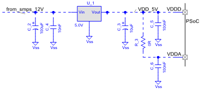
Be careful when using different LDOs to supply VDDD and VDDA. This could cause unnecessary issues. The reason there is a concern when directly connecting VDDD directly to VDDA is that sometimes the high-speed switching currents to clock logic in the digital domain can be seen as supply transients in the analog domain.
Here's a low-cost suggestion:
Each supply domain is de-coupled with a cap (C_5 and C_6). These caps MUST BE placed a close to the PSoC pins as physically possible. There is a 0 ohm resistor is a place-holder for a potential in-line ferrite bead inductor. As needed, you can replace the 0R with some in-line inductance to minimize VDDD switching influences on VDDA. If no inductance is needed, a 0 ohm resistor is very low cost. In this design, it shares 5V for VDDD and VDDA to use only one Vreg.
Len
"Engineering is an Art. The Art of Compromise."
