- Mark as New
- Bookmark
- Subscribe
- Mute
- Subscribe to RSS Feed
- Permalink
- Report Inappropriate Content
Hi,
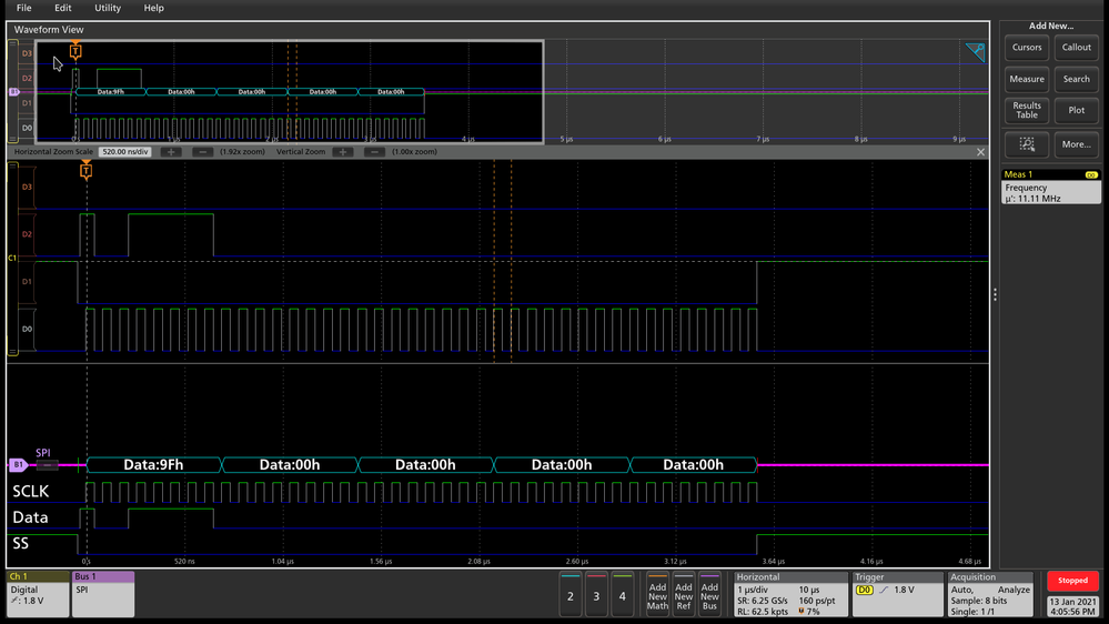
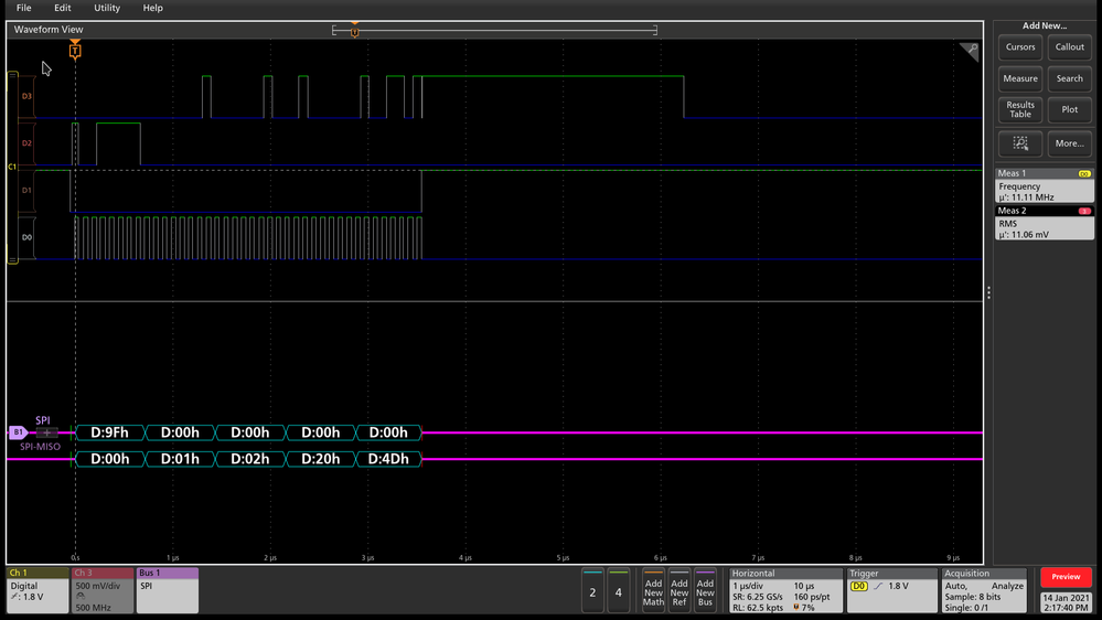
I am currently testing a S25FL512 flash. I am trying to test the read register function and sending a RDID command to the flash on SI (code 0x9F). However, I saw no response on SO and cannot read any data. (D0 to D3 are SCK, CS, SI and SO)

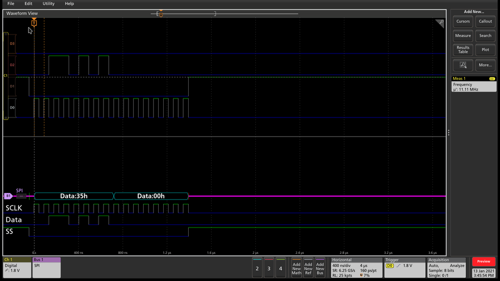
I then tried several other commands, including RDSR1 (05h) and RDCR (35h) nothing is appearing on SO signal.

I even tried toggling FLASH_RST signal to warm reset the device serval times, but it didn't help.
Currently I have no clue why this happen. Could anyone give me some hints or advice to understand what is the issue? Could that due to Power on Reset of the device?
P.S: My VCC and VIO are 3.3V, and VSS is at 0V. HOLD/RST/WP are grounded during the test.
Solved! Go to Solution.
- Labels:
-
Memory Nor Flash
- Mark as New
- Bookmark
- Subscribe
- Mute
- Subscribe to RSS Feed
- Permalink
- Report Inappropriate Content
I solved the problem this afternoon.
The issue is in the power up sequence. I didn't keep the CS high during the Power-up, as datasheet required:
The device must not be selected at power-up or power-down (that is, CS# must follow the voltage applied on VCC) until VCC reaches the correct value as follows
After fixing the Power up sequence, I can read the device ID successfully.

Actually, I found out the reason it not even this complicated. As @AS_36 mentioned, I shouldn't ground the HOLD# signal, since it will enter the HOLD mode and make SO high Z.
After raise the HOLD signal to 1 the problem is solved.
- Mark as New
- Bookmark
- Subscribe
- Mute
- Subscribe to RSS Feed
- Permalink
- Report Inappropriate Content
Hi,
Could you please explain the reason for grounding HOLD#, RESET# and WP# signals during the test? Table 2. of the datasheet mentions that these signals have an internal pull up resistor and may be left unconnected in the application if not required.
Regards.
- Mark as New
- Bookmark
- Subscribe
- Mute
- Subscribe to RSS Feed
- Permalink
- Report Inappropriate Content
Hi,
Thanks for your response. The WP, Hold and RST are actually mapped to FPGA output and can be High or low or floating. I have tried both floating and grounded, and there are no SO for both cases.
Do you think the issue can caused by those three pins? Is there any way I can check whether the Flash is powered up and ready for read?
Thanks
- Mark as New
- Bookmark
- Subscribe
- Mute
- Subscribe to RSS Feed
- Permalink
- Report Inappropriate Content
I solved the problem this afternoon.
The issue is in the power up sequence. I didn't keep the CS high during the Power-up, as datasheet required:
The device must not be selected at power-up or power-down (that is, CS# must follow the voltage applied on VCC) until VCC reaches the correct value as follows
After fixing the Power up sequence, I can read the device ID successfully.

Actually, I found out the reason it not even this complicated. As @AS_36 mentioned, I shouldn't ground the HOLD# signal, since it will enter the HOLD mode and make SO high Z.
After raise the HOLD signal to 1 the problem is solved.
- Mark as New
- Bookmark
- Subscribe
- Mute
- Subscribe to RSS Feed
- Permalink
- Report Inappropriate Content
Actually, I found out the reason it not even this complicated. As @Apurva_S mentioned, I shouldn't ground the HOLD# signal, since it will enter the HOLD mode and make SO high Z.
After raise the HOLD signal to 1 the problem is solved.