Non Volatile RAM (F-RAM & NVSRAM) Forum Discussions
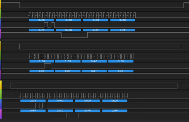
For better bus utilization on our system we use 32 bit width, including 32 bit spi transfer. It has the side effect that WEL opcode/command is sent as a 4 byte command which has worked fine in the past, using the FRAM device CY15B104Q. Now that we have changed to FRAM device CY15X108QI it does not work anymore. We have tried to have the WEL opcode first, last or fill all bytes, including having the other bytes as 0s, 1s or 55 which I think was mentioned as idle pattern, nothing makes the WEL latch when using 32 bit transfer. Sending the WEL opcode as a single byte works as expected, but is not how we would preferably do this.
The attached data is captured for the two devices using digital analyzer, and show
- read status register 0x5
- set write enable latch 0x6
- read status register 0x5 again to see if WEL was set or not
CY15B104Q accepting 32 bit transfer for WEL:

CY15X108QI not accepting 32 bit transfer for WEL:
Is it, should it be possible? It worked in the past for other chip? Please advice.
Show LessDear Cypress-Community,
we use the FRAM FM28V020-SG since over 10 years, and we had no problems for a long time. In this fine working time period we use FM28V020-SG with second number e.g. "A 1601602287" or older...
But since end of 2018 the FM28V020-SG with second number G 1749647029 makes more and more problems.
Since April 2020 5% of our boards with FM28V020 lost some bytes (we are always testing the F-RAM Memory each 2seconds --> we get checksum errors since FM28V020-SG with seconde number G 1749647029).
Can you say me, what has changed from older to newer FM28V020-SG Versions ?
Does something was changed in the Maximum Ratings? Or was there a change in the operating range?
Or was there a change in the timing? Or anything else?
Thanks a lot for your answer(s).
Best regards
Markus T. from Germany
Show LessDear Support team,
FRAM FM25V10 datasheet mentions that the device specifications are guaranteed over an industrial temperature range of –40°C to +85°C. But under maximum ratings section Ambient temperature range with power applied is mentioned to be –55°C to +125°C. I was wondering whether it is possible to operate this FRAM above 85°C upto 125°C? Will it behave in the same manner as specified in the datasheet, in this case?
Thanking you in advance.
Show LessHello,
I am using the Verilog Simulation Model of the FM24V10 (FM24V10 - VERILOG.zip (cypress.com)) and encountered the following problem: TheSimulation model seems to have a write buffer of 128 bytes, see line 80 of file FRAM_I2C.v:
reg [07:00] WrDataByte [0:127]; // memory write data buffer
Hence, sending datagrams of length > 128 Bytes result in data loss. However, I can not find any information regarding a size limitation of writes in the datasheet (FM24V10, 1-Mbit (128K × 😎 Serial (I2C) F-RAM (cypress.com)).
Can anyone confirm that there is mismatch between datasheet and model? Does the device have a writebuffer of size 128 byte?
Thank you. Best regards
Jan
Show Less
Datasheet says "2.6 mA (typ) active current at 40 MHz." Does the current scale with frequency? What would be the current for 8bit data at 1kHz?
Also, would FRAM be MRI safe?
Show LessAre there any shock and vibration test data for the F-ram product line?
I want to use several 8Mbit x8 SPI 40MHz Excelon LP F-RAM devices in an application where I need to convert signals coming from a parallel x8 SRAM interface to 40MHz SPI signals and also 40MHz SPI signals sourced from the SPI F-RAM device to signals destined for the x8 parallel SRAM interface. As for the x8 parallel SRAM interface timings, conservatively, I have a memory address setup time of around 250ns, a memory address hold time of around 1250ns and a chip enable hold time of around 750ns ( I'm not quite sure of the timings right now and I know I am missing some timing information for some of the x8 parallel SRAM signals ). I plan on doing this with an ultra-low-power MCU, but, I'd need to use cycle-stretching on the Cypress F-RAM device(s). Is the above kind of conversion doable, especially the cycle stretching?
( N.B. The devices I want to use are one of these : https://www.cypress.com/file/444186/download , https://www.cypress.com/file/444186/download )
Thanks,
jdb2
Show LessIs there any data, reports, etc for SEU info on the CY15B104q devices?
Thanks
Danny
Check out the Article "Ensuring fail-safe data storage in battery-powered IoT sensor nodes".
In this article, we will examine the often neglected but most important aspect of any sensor node – local memory.
F-RAM, such as the Excelon F-RAM from Cypress, addresses all concerns related to memory, making it highly efficient for IoT-based data logging. F-RAM endurance is 10^14 write/read cycles and provides immediate non-volatility and byte accessibility. Its low write/read current of 2.4mA, standby current of 2.3uA and hibernate current of 0.1uA, yield extremely low power such as is required for battery-operated IoT devices.
Show Less