- Mark as New
- Bookmark
- Subscribe
- Mute
- Subscribe to RSS Feed
- Permalink
- Report Inappropriate Content
We are using a Cypress/Infineon HyperRAM, part number S70KS1281DPBHV020, driven by the Cypress/Infineon Hyperbus Controller on a Xilinx FPGA (xc7k160t-2ffg676) at 100 MHz. On said FPGA is also a soft-microcontroller (MicroBlaze) that uses the HyperRAM as instruction memory.
We have issues with erratic behaviour of the MicroBlaze after some time passes, usually several days. When we read back the processor’s instruction memory we see that entire blocks have been corrupted. We see that the corrupt blocks are 1024 bytes in size and are located at offsets of 1024 bytes as well. According to the HyperRAM component’s datasheet, the RAM is organized in 16384 rows of 1024 bytes. It appears that the corrupt memory blocks all contain the same data after the fact.
We have ensured that no write access has taken place to the instruction memory, so it must have changed spontaneously. We have also verified that we do not violate the RAM's tCMS and are also providing additonal latency for refresh cycles with every single access. As far as we know, the FPGA drives the HyperRAM according to specifications.
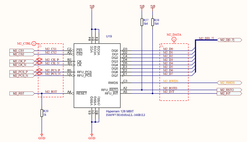
We have reviewed our schematics and have noticed a few issues that however don't seem to be very critical:
- We have added pull up resistors on the pins A2 (RSTO#) and A5 (INT#), which are marked as “RFU” in the HyperRAM datasheet. In the FPGA, they are unused so there is a weak pull-down (10-40k if I’m not mistaken) by default. In the Documentation of the Infineon/Cypress/Spansion HyperBus Controller, I found the following passage regarding the INT and RSTO pins, which might be the reason we have added those:
- On the A4 pin (RESET#), we have a pull down resistor, but in the datasheet, Cypress/Infineon indicates that there is an internal weak pull up resistor in the HyperRAM. During normal operation, this signal is driven by the FPGA, however.
- The B5/C5 pins (PCS/PCS#) are RFU in the datasheet as well but are unconnected in the FPGA, which means there is a weak pulldown there as well.
- The C2 pin (CS1) is RFU in the datasheet but driven high by the FPGA.
- We have also noticed that our Power Delivery trace widths are 11.8 mils wide, which is below the recommended 20 mils in the Design Guide you’ve sent.
We are driving the CK/CK# as two phase-shifted clocks, not through a differential buffer as the schematics might suggest. The schematics also show an ISSI HyperRAM part, but we are experiencing the exact same issue with that one.
What could be the cause of this?
- Mark as New
- Bookmark
- Subscribe
- Mute
- Subscribe to RSS Feed
- Permalink
- Report Inappropriate Content
Hi,
We will need to understand the issue better before commenting on it. If you are okay to share each details on public forum we can continue the debug process here or if you want we can move to case system where everything will be kept confidential if you are not comfortable to share the details on public platform.
In addition to the schematics
1) We will need more details on the failure. Can you provide us the dump file for data. One of correct data and second of corrupted data.
2) Can you let us know how many devices are showing this behavior.
3) What is operating temperature
4) Can you let us know the values for SR and CR.
5) Can you provide us scope shot for a power up on the device, a read operation and a write operation. Just want to ensure that all the timing specifications are met.
Thanks,
Pradipta.
- Mark as New
- Bookmark
- Subscribe
- Mute
- Subscribe to RSS Feed
- Permalink
- Report Inappropriate Content
Hi,
Moving this to Support case for further discussions.
Thanks,
Pradipta.
