Feb 24, 2020
12:49 PM
- Mark as New
- Bookmark
- Subscribe
- Mute
- Subscribe to RSS Feed
- Permalink
- Report Inappropriate Content
Feb 24, 2020
12:49 PM
Hello everyone, I use the gate driver ic IR2136, when I measure between VB1 and VS1 I haven't 15V, I have to put the source pin of the mosfet transistor at the GND to have a potential difference of 15V between VB1 and VS1.
i look at the page 5 of the datasheet of the IR2136 to help me
the values of the components : 1) 3x diodes 1N4007
2) 5x 1kohm resistors
3) 6x 1µF capacitors
4) mosfet STP43N60DM2
if someone has already worked on a circuit like this ? please give me some tips to correct this error.
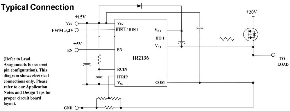

i look at the page 5 of the datasheet of the IR2136 to help me
the values of the components : 1) 3x diodes 1N4007
2) 5x 1kohm resistors
3) 6x 1µF capacitors
4) mosfet STP43N60DM2
if someone has already worked on a circuit like this ? please give me some tips to correct this error.


Solved! Go to Solution.
Labels
- Labels:
-
ispn:10207:1:0
-
l1:144:1:0
-
l2:1244:1:0
- Tags:
- IFX
1 Solution
May 06, 2020
07:28 AM
- Mark as New
- Bookmark
- Subscribe
- Mute
- Subscribe to RSS Feed
- Permalink
- Report Inappropriate Content
May 06, 2020
07:28 AM
Hi, I have determined the values of my components but I'm not sure that the calculation is good.
Can someone check my calculations please ?
bootstrap capacitor : 47nF
bootstrap diode : BA218
bootstrap resistance : 100 ohms
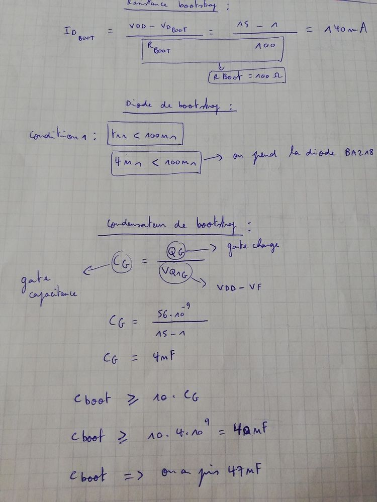
and the documents of the calculations :
http://www.ti.com/lit/an/slua887/slua887.pdf?ts=1588775387752
https://www.infineon.com/dgdl/Infineon-Using_Monolithic_Voltage_Gate_Drivers-AN-v01_00-EN.pdf?fileId...
Can someone check my calculations please ?
bootstrap capacitor : 47nF
bootstrap diode : BA218
bootstrap resistance : 100 ohms

and the documents of the calculations :
http://www.ti.com/lit/an/slua887/slua887.pdf?ts=1588775387752
https://www.infineon.com/dgdl/Infineon-Using_Monolithic_Voltage_Gate_Drivers-AN-v01_00-EN.pdf?fileId...
11 Replies
Feb 25, 2020
02:24 AM
- Mark as New
- Bookmark
- Subscribe
- Mute
- Subscribe to RSS Feed
- Permalink
- Report Inappropriate Content
Feb 25, 2020
02:24 AM
here I tested with a diode 1N4148, I configured my PWM at 1Hz, I checked that my transistor switches every second, I put a load resistance of 82 ohm / 5W and I measured 14.61V between VB-S, the problem now is that my load resistance starts to heat up a lot when I increase the frequency of my PWM.
Attachments are accessible only for community members.
Feb 25, 2020
10:26 AM
- Mark as New
- Bookmark
- Subscribe
- Mute
- Subscribe to RSS Feed
- Permalink
- Report Inappropriate Content
Feb 25, 2020
10:26 AM
Hi,
Are you providing inputs for low side gate driver outputs? If so, what is their duty cycle? The bootstrap capacitor gets charged when the low side MOSFET turns on. Pls review the attached application notes to get a better understanding of how these IC's operate.
You dont have to connect a load resistor.
Feb 25, 2020
11:51 AM
- Mark as New
- Bookmark
- Subscribe
- Mute
- Subscribe to RSS Feed
- Permalink
- Report Inappropriate Content
Feb 25, 2020
11:51 AM
Srivatsa wrote:
Hi,
Are you providing inputs for low side gate driver outputs? If so, what is their duty cycle? The bootstrap capacitor gets charged when the low side MOSFET turns on. Pls review the attached application notes to get a better understanding of how these IC's operate.
You dont have to connect a load resistor.
yes I have put 3V3 PWM at LIN1 and the duty cycle is at 50%
here is the tests that I did at 1kHz : 1) High Side

2) Low Side

load resistance is 82ohm / 5W
infact I want to realize a Sine PWM signal at the output of the transistor bridges to be able to drive an asynchronous motor
the problem is that I don't know how to achieve a reverse PWM for the Low Side
at the end it will be necessary that I have a signal on each motor phase which looks like this:

Feb 26, 2020
10:23 AM
- Mark as New
- Bookmark
- Subscribe
- Mute
- Subscribe to RSS Feed
- Permalink
- Report Inappropriate Content
Feb 26, 2020
10:23 AM
Please share your schematics.
Feb 26, 2020
12:42 PM
- Mark as New
- Bookmark
- Subscribe
- Mute
- Subscribe to RSS Feed
- Permalink
- Report Inappropriate Content
Feb 26, 2020
12:42 PM
Srivatsa wrote:
Please share your schematics.
the schematic :

Feb 27, 2020
10:48 AM
- Mark as New
- Bookmark
- Subscribe
- Mute
- Subscribe to RSS Feed
- Permalink
- Report Inappropriate Content
Feb 27, 2020
10:48 AM
The 82 ohm is not needed in actual application. You are using it to charge the bootstrap capacitor which provides HO output. Ideally when LO turns on the low side MOSFET, the bootstrap capacitor should get charged.
Pls connect the VS 1,2,3 node to motor windings. To generate the required PWM pattern kindly check with the respective micro-controller application support teams who can help you with the algorithms.
You can look at Infineon's Digital Motor Controller (iMOTION™) solution and perform simulations at https://plex.infineon.com/plexim/ipmmotor.html
Attachments are accessible only for community members.
Feb 29, 2020
03:33 AM
- Mark as New
- Bookmark
- Subscribe
- Mute
- Subscribe to RSS Feed
- Permalink
- Report Inappropriate Content
Feb 29, 2020
03:33 AM
Srivatsa wrote:
The 82 ohm is not needed in actual application. You are using it to charge the bootstrap capacitor which provides HO output. Ideally when LO turns on the low side MOSFET, the bootstrap capacitor should get charged.
Pls connect the VS 1,2,3 node to motor windings. To generate the required PWM pattern kindly check with the respective micro-controller application support teams who can help you with the algorithms.
You can look at Infineon's Digital Motor Controller (iMOTION™) solution and perform simulations at https://plex.infineon.com/plexim/ipmmotor.html
Hello, I made new measurements by connecting all the transistor bridge, the low side works but the high side does not work.
I also noticed that I don't have the 15V at the VB1 - VS1 terminals, instead I have around 500mV.
wiring diagram :
high side probe :

low side probe :

PS: the capacitors are badly rated, they are all 1µF
and the PWM operates at 500 Hz
Mar 03, 2020
10:57 AM
- Mark as New
- Bookmark
- Subscribe
- Mute
- Subscribe to RSS Feed
- Permalink
- Report Inappropriate Content
Mar 03, 2020
10:57 AM
Pls check if the MOSFET Q8 is turning ON. Also, check the status of Fault pin. You can write to me at srivatsa.raghunath@infineon.com and I will see if I can get a field applications engineer to support you onsite.
Mar 10, 2020
01:00 AM
- Mark as New
- Bookmark
- Subscribe
- Mute
- Subscribe to RSS Feed
- Permalink
- Report Inappropriate Content
Mar 10, 2020
01:00 AM
Srivatsa wrote:
Pls check if the MOSFET Q8 is turning ON. Also, check the status of Fault pin. You can write to me at srivatsa.raghunath@infineon.com and I will see if I can get a field applications engineer to support you onsite.
Hello, I determined the value of the capacitor, it is 33nF, I am doing tests and I now have a PWM from 0 to 20V in VS1, VS2 and VS3.
the problem now is that I have current spikes at each switching, I tried to put a big filtering condo on the 20V power supply and this has reduced the spikes but there are still some left.
Mar 11, 2020
07:37 AM
- Mark as New
- Bookmark
- Subscribe
- Mute
- Subscribe to RSS Feed
- Permalink
- Report Inappropriate Content
Mar 11, 2020
07:37 AM
For reducing the current spikes, you can check your layout. See an optimal layout example as attached. Use dedicated traces right from the shunt resistor to the resistors of
amplifier. Traces must not be shared with ground planes. Keep traces among MOSFETs and DC bus capacitors as short as possible.
You can also try with a bigger Vcc capacitor.

amplifier. Traces must not be shared with ground planes. Keep traces among MOSFETs and DC bus capacitors as short as possible.
You can also try with a bigger Vcc capacitor.

May 06, 2020
07:28 AM
- Mark as New
- Bookmark
- Subscribe
- Mute
- Subscribe to RSS Feed
- Permalink
- Report Inappropriate Content
May 06, 2020
07:28 AM
Hi, I have determined the values of my components but I'm not sure that the calculation is good.
Can someone check my calculations please ?
bootstrap capacitor : 47nF
bootstrap diode : BA218
bootstrap resistance : 100 ohms

and the documents of the calculations :
http://www.ti.com/lit/an/slua887/slua887.pdf?ts=1588775387752
https://www.infineon.com/dgdl/Infineon-Using_Monolithic_Voltage_Gate_Drivers-AN-v01_00-EN.pdf?fileId...
Can someone check my calculations please ?
bootstrap capacitor : 47nF
bootstrap diode : BA218
bootstrap resistance : 100 ohms

and the documents of the calculations :
http://www.ti.com/lit/an/slua887/slua887.pdf?ts=1588775387752
https://www.infineon.com/dgdl/Infineon-Using_Monolithic_Voltage_Gate_Drivers-AN-v01_00-EN.pdf?fileId...