- Mark as New
- Bookmark
- Subscribe
- Mute
- Subscribe to RSS Feed
- Permalink
- Report Inappropriate Content
Hi, I am trying to establish the rise time of the 1ED3142 gate driver @ Vvcc-Vvee = 20V.
The data sheet states 20nS maximal rise time but no minimum or typical Value. I would like to achieve as short a rise time as the mosfet will allow , if possible.
Input capacitance of the Mosfet is 579pF, gate charge is 37nC, rise time is 8nS.
The function generator has a 7ns rise time output signal.
What will be the probably output rise time of the 1ED3142 gate driver?
Thank you
eccone
Solved! Go to Solution.
- Tags:
- 1ED3142 gate driver
- Mark as New
- Bookmark
- Subscribe
- Mute
- Subscribe to RSS Feed
- Permalink
- Report Inappropriate Content
Hi,
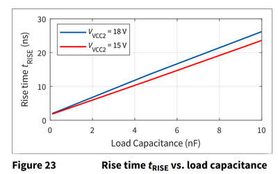
The typical rise time with respect to capacitive loading is given in page-16 of the datasheet
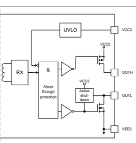
To get this curve, a capacitive load is placed at the output of GD (OUTH)in the dynamic test circuit. It would look like a typical RC circuit (R is Rds,on of PMOS) and will take appropriate time to reach to VCC level as per capacitance value
Now, if you consider the practical application, where you would be switching a MOSFET then you would be charging C_GS of the MOS through a particular gate resistor value (based on device dv/dt limitation). The rise time will entirely depend upon the gate resistor value and MOS gate to source capacitance in addition to it C_GD would also be playing major role in deciding the width of plateau region. Overall your rise time will going to be on the higher side compare to what mentioned in the datasheet for a particular capacitive loading.
Regards,
Rishabh
- Mark as New
- Bookmark
- Subscribe
- Mute
- Subscribe to RSS Feed
- Permalink
- Report Inappropriate Content
Hi,
Good day!
Sorry, I could not properly understand your question
- What is the 8ns MOSFET rise time?
- As you gave all the data i.e. function gen rise time, are you asking for the total time taken from function gen input up till gate driver output transition (including prop delay) or you are asking for MOS gate voltage transition.
Regards,
Rishabh
- Mark as New
- Bookmark
- Subscribe
- Mute
- Subscribe to RSS Feed
- Permalink
- Report Inappropriate Content
Good day Rishabh,
Thank you kindly for replying. No, I am not interested in the propagation delays and transitions but the 'on' rise time matching of the function generator signal and the Mosfet - dv/dt .
Preferably I'd like to achieve a 7nS rise time pulse from the function generator replicated as a 7nS rise time of the driver output to the gate of the Mosfet.
I hope this a bit less foggy.
Regards
ecc
- Mark as New
- Bookmark
- Subscribe
- Mute
- Subscribe to RSS Feed
- Permalink
- Report Inappropriate Content
Hi,
The typical rise time with respect to capacitive loading is given in page-16 of the datasheet
To get this curve, a capacitive load is placed at the output of GD (OUTH)in the dynamic test circuit. It would look like a typical RC circuit (R is Rds,on of PMOS) and will take appropriate time to reach to VCC level as per capacitance value
Now, if you consider the practical application, where you would be switching a MOSFET then you would be charging C_GS of the MOS through a particular gate resistor value (based on device dv/dt limitation). The rise time will entirely depend upon the gate resistor value and MOS gate to source capacitance in addition to it C_GD would also be playing major role in deciding the width of plateau region. Overall your rise time will going to be on the higher side compare to what mentioned in the datasheet for a particular capacitive loading.
Regards,
Rishabh
- Mark as New
- Bookmark
- Subscribe
- Mute
- Subscribe to RSS Feed
- Permalink
- Report Inappropriate Content
Good day Rishabh,
Thank you very much for your answer. That was helpful.
Kind regards
ecc

