- Mark as New
- Bookmark
- Subscribe
- Mute
- Subscribe to RSS Feed
- Permalink
- Report Inappropriate Content
Design Considerations
Sensor Construction
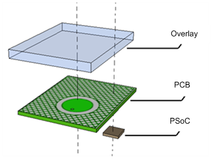
A capacitive sensor can be constructed using different materials depending on the application requirements. In a typical sensor construction, a conductive pad, or surface that senses a touch is connected to pin of PSoC MCUs using a conductive trace or ink. This arrangement is placed below a non-conductive overlay material and the user interacts on the top of the overlay
Typical CapSense Sensor Construction
The copper pads etched on the surface of the PCB act as CapSense sensors. A nonconductive overlay serves as the touch surface. The overlay also protects the sensor from the environment and prevents direct finger contact. A GND hatch surrounding the sensor pad isolates the sensor from the other sensors and PCB traces. The simplest CapSense PCB design is a two-layer board with sensor pads and hatched GND plane on the top layer, and the electrical components on the bottom layer.
CapSense Hardware
Overlay Selection
The overlay is an important parameter of a CapSense system, as it determines the magnitude of finger capacitance. The finger is directly proportional to the relative permittivity of the overlay material. This table shows the relative permittivity of some common overlay materials. Materials with relative permittivity between 2.0 and 8.0 are well suited for CapSense overlays.
NOTE: conductive materials interfere with the electric field pattern. Therefore, use of conductive overlay materials is not recommended.
Relative Permittivity of Overlay Materials
Material | er |
|---|---|
Air | 1.0 |
Formica | 4.6 – 4.9 |
Glass (Standard) | 7.6 – 8.0 |
Glass (Ceramic) | 6.0 |
PET Film (Mylar®) | 3.2 |
Polycarbonate (Lexan®) | 2.9 – 3.0 |
Acrylic (Plexiglas®) | 2.8 |
ABS | 2.4 – 4.1 |
Wood Table and Desktop | 1.2 – 2.5 |
Gypsum (Drywall) | 2.5 – 6.0 |
Overlay Thickness
Finger capacitance is inversely proportional to the overlay thickness. Therefore, a thin overlay gives more signal vs. a thick overlay. This table lists the recommended maximum thickness of acrylic overlays for different CapSense sensor types.
Because finger capacitance also depends on the dielectric constant of the overlay, the dielectric constant also plays a role in the guideline for the maximum thickness of the overlay. Common glass has a dielectric constant of approximately εr = 8, while acrylic has approximately εr = 2.5. The ratio of εr/2.5 is an estimate of the overlay thickness relative to plastic for the same level of sensitivity. Using this rule of thumb, a common glass overlay can be about three times as thick as a plastic overlay while maintaining the same level of sensitivity.
For CSX sensing, it is recommended to have minimum overlay thickness of 0.5 mm.
Maximum Thickness of Acrylic Overlay
Widget | Maximum Thickness (mm) |
|---|---|
Button | 5 |
Slider | 5 |
Touchpad | 0.5 |
Overlay Adhesives
The overlay must have a good mechanical contact with the PCB. You should use a nonconductive adhesive film for bonding the overlay and the PCB. This film increases the sensitivity of the system by eliminating the air gap between the overlay and the sensor pads. 3M™ makes a high-performance acrylic adhesive called 200MP that is widely used in CapSense applications. It is available in the form of adhesive transfer tapes; example product numbers are 467MP and 468MP.
To find out more, please check the PSoC 4 and PSoC 6 MCU CapSense Design Guide.

